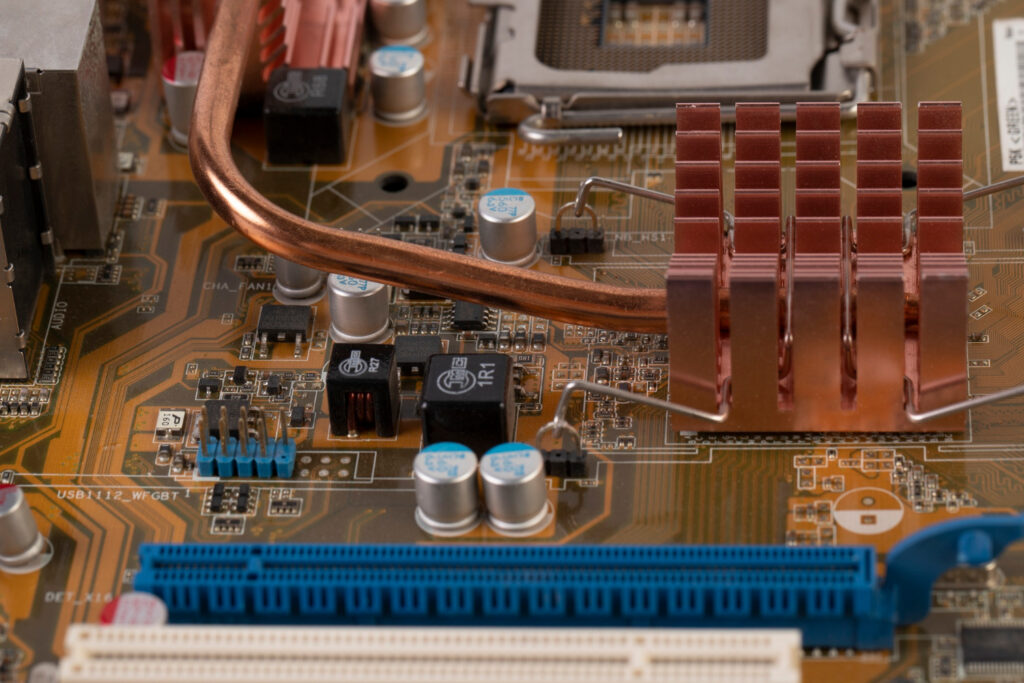
Custom IC Design
ASIC Design:
Delivering comprehensive solutions using custom-built ASIC with exceptional performance, power, area efficiency, and reliability tailored to your specific application needs
FPGA Design:
Providing versatile FPGA design services, enabling rapid prototyping and deployment of complex digital circuits. Our expertise ensures seamless integration, high- speed performance, and adaptability for evolving requirements.
Design for Testability (DFT)
Integrating advanced techniques like SSN, BIST and memory repair, ensuring comprehensive fault detection and efficient testing. By implementing robust DFT methodologies, we enhance the manufacturability, yield, and long-term reliability of your integrated circuits, ensuring high-quality production
Analog and Mixed-Signal Design:
Circuit Design:
Our analog circuit design services provide high-performance, low-noise, and power-efficient solutions tailored to meet stringent application requirements. Leveraging advanced techniques and tools, we deliver optimized analog circuits that ensure superior functionality, reliability, and manufacturability
Analog and Std cell Layout:
Our layout design services ensure precise, low-noise analog layouts and highly area optimized standard cell designs for superior circuit performance. Utilizing cutting-edge tools and methodologies, we deliver robust, manufacturable layouts that enhance reliability, and integration within your chip design
Mixed-Signal Integration:
Our Mixed Signal Integration expertise ensures smooth and efficient merging of analog and digital components, delivering cohesive and seamless integration for Analog Mixed Signal (AMS) designs


Digital Design:
RTL Design and Synthesis:
Our services leverage advanced methodologies and tools to translate high-level design concepts into optimized Register Transfer Level (RTL) descriptions, ensuring efficient logic implementation. We specialize in synthesizing complex digital designs, focusing on maximizing performance, minimizing area utilization, and achieving timing closure for rapid integration and reliable operation in integrated circuits
Low-Power Design Techniques:
Our low-power design techniques integrate advanced methodologies at various levels to minimize power consumption while maintaining high performance and reliability in integrated circuits. Leveraging state-of-the-art tools, we specialize in optimizing power distribution, implementing power gating, and reducing leakage currents to extend battery life and enhance overall energy efficiency
Physical Design:
Floorplanning:
We specialize in balancing utilization and power distribution, optimizing floorplans for low power to enhance manufacturability and meet stringent performance targets at block and full chip level
Placement and Routing:
We specialize in routing complex interconnections efficiently, ensuring signal integrity, timing closure, and manufacturability for high-density integrated circuits


Post-Layout Optimization:
Static Timing Analysis:
Our STA services use industry standard tools and methodologies to accurately assess timing paths and address timing violations early in the design phase, ensuring optimized performance and minimizing risks in performance and testing.
Power and Signal Integrity Analysis:
By identifying and mitigating power noise and signal integrity issues early in the design cycle, we optimize for power, performance, enhance overall reliability of your designs and ensure stable power distribution and signal integrity
Physical Verification and Sign off:
Our services employ the latest tools and rigorous checks to ensure layout accuracy and adherence to complex DRC and DFM rules. We ensure your designs meet stringent quality standards and are ready for fabrication.
Design Verification and Validation:
Functional Verification
- Lyptus offers a comprehensive suite of services in the domain of Design Verification
- Resources with specialized skillsets in creating verification environments from scratch-up using advanced methodologies.
- Ability to take full ownership and deliver bug free RTL Design
- Design Verification team specialized in IP/Block level, Subsystem (Cluster) level, and SoC level verification closure with all the quality metrics.
- Well thought out pyramid team driven by seasoned senior Design Verification architects to take up work of any complexity.
- Proven experience is defining the test bench architecture, verification plan, documentation, re-usable and modular test bench.
- Verification Planning:
- Feature Extraction
- Stimulus Generation
- Coverage
- Checkers
- Bug rate, Code, Functional and Assertion coverage driven
- Hands-on experience in niche protocols:
- ARM
- DDR
- Ethernet
- PCIe
- CXL
- JTAG
- NOC
- DEBUG IP
- HS IO
- Hands-on experience in the integration of third-party Verification IP’s into the test bench
- Ability to handle Small – Medium – Large sized Turnkey projects as well as cater to staff augmentation-based projects
- Well defined process and curriculum to train young engineers on the basics of functional verification, HDL’s and HVL’s, advanced verification methodology (such as SV/UVM), and protocols such Ethernet, PCIe etc
- Hands-on experience in niche protocols:
- IP / Sub System/SoC level verification
- Functional Validation Automation
- Mixed Signal
- Low Power – Power aware
- Gate Level Simulation
- Coverage closure
Emulation:
- Emulation model build and validation
- Emulation environment set up
- Porting the design on emulators
- Emulation using ZEBU, Palladium, Velloce
Formal Verification:
- Formal Verification using industry standard tools
- Feasibility study of the design to understand if the design is conducive for Formal Verification
- Experience team for Planning, Implementation, Execution
Low Power and Gate Level Simulations:
- Experienced team in low power and power aware simulations (UPF), Zero/Unit delay Gate level simulations, SDF back-annotated netlist simulations
- Environment setup and verification
Design for Testability (DFT):
- DFT Architecture & Implementation
- MBIST insertion and validation
- JTAG and Boundary scan
- ATPG – Pattern generation, simulation, coverage improvement, fault checks, DRCs
- Scan insertion and simulation
- SSN
- Test Access Port